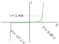
In a p-n junction diode, the reverse bias can be increased until the depletion layer breaks down and the diode suffers permanent damage. In a Zener diode, this does not happen because of a highly doped p-n junction. In a highly doped junction, the conduction and valence bands on opposite sides of the junction are sufficiently close during reverse bias such that electrons may tunnel directly from the valence band on the p-side into the conduction band on the n-side. When the reverse bias voltage passes beyond a critical magnitude known as the breakdown or Zener voltage, the entire depletion area is filled by the electrons migrating from the p to n-part of the barrier and any attempt to increase the voltage drop across the barrier is virtually unsuccessful.
 |
| Photo ByFilip Dominec |
The useful function is that the potential difference across the diode remains constant at VZ, over a wide range of reverse currents (i.e. the breakdown current part of the characteristic is nearly at right angles to the VR axis). It is this property of a Zener diode that makes it useful in stabilising power supplies, keeping the voltage output steady.