The p–n Junction
Explain how a p–n junction forms a depletion region and why it conducts under forward bias but not under reverse bias (A Level Physics).
Continue where you stopped
The core idea
On this page
Learning objectives
- Explain p-n junction formation and bias, and analyse diode, LED, Zener, rectifier-smoothing, sensor and transistor-switching circuits.
1. Definitions (Must Know)
A. p–n junction
A p–n junction is formed when p-type and n-type semiconductors are joined together.
It conducts easily in one direction (forward bias) but not the other (reverse bias).
B. Depletion region
The depletion region is the region near the junction where mobile charge carriers are depleted (few free electrons/holes).
It contains fixed ions:
- positive donor ions on the n-side (where electrons have diffused away)
- negative acceptor ions on the p-side (where holes have been filled)
C. Forward bias and reverse bias
- Forward bias: p-side connected to the positive terminal, n-side to the negative terminal.
- Reverse bias: p-side connected to the negative terminal, n-side to the positive terminal.
2. Key Ideas (What Earns Marks)
- When a p–n junction forms, electrons and holes diffuse across the junction and recombine, leaving fixed ions behind → depletion region.
- The depletion region creates an electric field (potential barrier) that opposes further diffusion.
- Forward bias reduces the barrier and depletion width → significant current can flow.
- Reverse bias increases the barrier and depletion width → current is (approximately) zero (ignoring small leakage).
Forward bias: p to +, n to −. Reverse bias: p to −, n to +.
3. Detailed Explanations
A. How the depletion region forms
Before contact:
- n-type has many electrons (majority carriers)
- p-type has many holes (majority carriers)
After contact:
- electrons diffuse from n to p and recombine with holes
- holes effectively diffuse from p to n (equivalently, electrons move the other way and fill holes)
Recombination near the junction removes mobile carriers and leaves behind fixed dopant ions, creating the depletion region.
B. Why the junction blocks current without forward bias
The fixed ions create an electric field that pushes:
- electrons back towards the n-side
- holes back towards the p-side
This opposes further diffusion. At equilibrium, diffusion and drift balance, so there is no net current.
C. Reverse bias (why current is small)
Reverse bias pulls:
- electrons towards the positive terminal on the n-side
- holes towards the negative terminal on the p-side
This widens the depletion region and strengthens the barrier, so majority carriers cannot cross the junction.
D. Forward bias (why current is large)
Forward bias pushes:
- electrons towards the junction from the n-side
- holes towards the junction from the p-side
This reduces the depletion width and barrier, allowing carriers to cross and a significant current to flow.
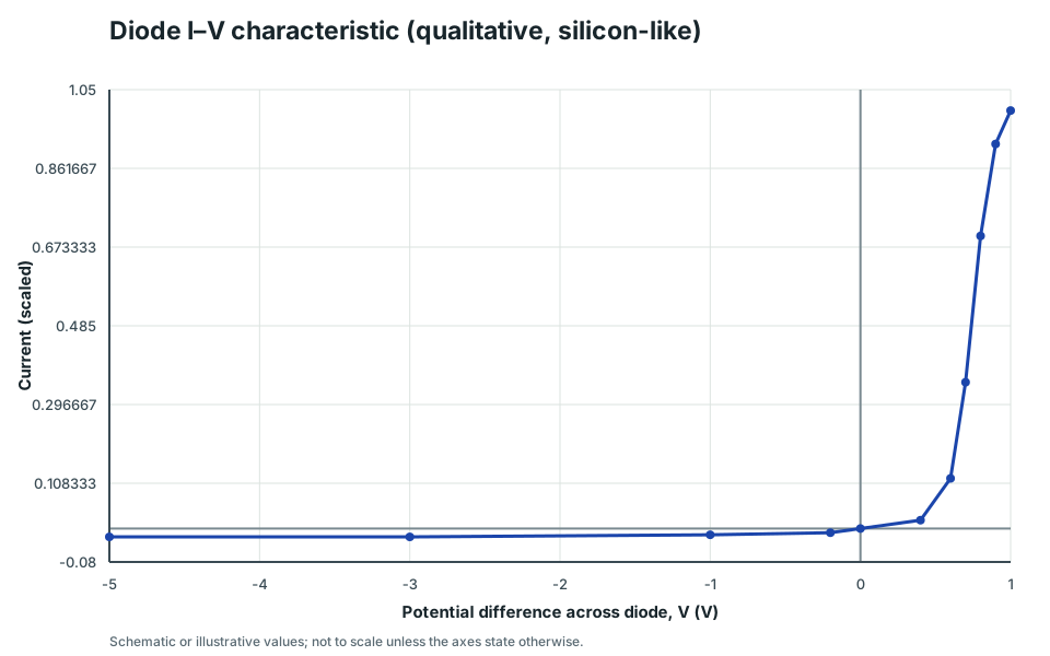
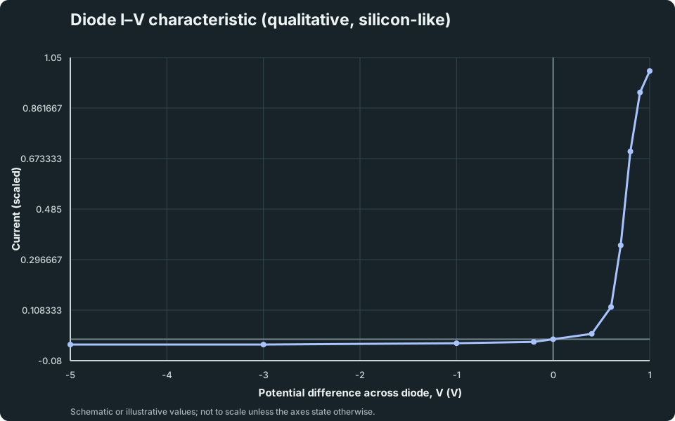
Diode I–V characteristic (qualitative, silicon-like)
A qualitative I–V curve: tiny reverse leakage current and a steep rise in forward current beyond about 0.7 V.
Scroll across the graph to read all labels.
View figure data
| Potential difference across diode, V (V) | Diode I–V (schematic) |
|---|---|
| -5 | -0.02 |
| -3 | -0.02 |
| -1 | -0.015 |
| -0.2 | -0.01 |
| 0 | 0 |
| 0.4 | 0.02 |
| 0.6 | 0.12 |
| 0.7 | 0.35 |
| 0.8 | 0.7 |
| 0.9 | 0.92 |
| 1 | 1 |
4. Common Mistakes
- Swapping the forward and reverse bias connections.
- Saying “no current” in reverse bias without noting “approximately” (there can be small leakage).
- Thinking the depletion region contains lots of free charges (it contains mostly fixed ions).
5. Exam Tips
- Use a labelled diagram: show p-side, n-side, and battery polarity.
- State what happens to depletion width (increases for reverse bias, decreases for forward bias).
- If the question moves to circuit behaviour, link to the diode I–V characteristic (covered in the circuits topic).
Use the Semiconductor Devices Lab to compare depletion width under forward and reverse bias, then connect that model to diode conduction and rectification.
6. Worked Examples
Modelled example 1
Identify the bias condition
Problem
Study the worked solution
Match the polarity
Method
The junction is reverse biased.Reason
Reverse bias connects p to negative and n to positive.Working
p → -; n → +Track majority carriers
Method
Electrons and holes are pulled away from the junction.Reason
The applied field drives n-side electrons towards the positive terminal and p-side holes towards the negative terminal.Working
majority carriers move away from junctionInfer the junction state
Method
The depletion region widens and current is approximately zero, apart from small leakage.Reason
The potential barrier increases and blocks majority-carrier crossing.Working
w_depletion↑ ⇒ I ≈ 0
Common misconception 2
Current direction in forward bias
Learner claim
Try this before viewing the solution
View solution step by step
Separate electron drift
Method
Electrons crossing from n towards p move opposite to conventional current.Reason
Electrons carry negative charge.Working
vector I opposite vector vₑTrack holes
Method
Holes move from p towards n and behave as positive carriers.Reason
Their effective drift direction matches conventional current.Working
vector vₕ parallel to vector ICorrect the direction
Method
Conventional current flows from the p-side to the n-side through the forward-biased diode.Reason
Both carrier descriptions correspond to that same conventional-current direction.Working
p → n
7. Mind Stretchers
Mind stretcher 1: Question 1Extension
Explain why forward bias can lead to a large current even though the depletion region exists.
Show Answer
Forward bias reduces the potential barrier and narrows the depletion region. Majority carriers are pushed towards the junction and can cross it more easily, so the current increases greatly.
Mind stretcher 2: Question 2Extension
Why does reverse bias not “suck” electrons across the junction and create current?
Show Answer
Reverse bias increases the barrier and widens the depletion region, so majority carriers cannot cross. Only a small leakage current (due to minority carriers) may flow, which is usually negligible in basic circuit questions.
8. Optional (Enrichment)
A. Diode equation (beyond typical A Level needs)
Real diode I–V behaviour can be modelled with an exponential relationship (Shockley diode equation). A Level questions typically focus on direction, approximate conduction/blocking, and I–V graph interpretation rather than deriving the equation.