Zener Diode
Key idea: H3 Solid State Physics: Zener Diode — key ideas and exam-focused notes on bonding, crystal structures, conduction models, and band ideas.
Continue where you stopped
The core idea
On this page
Learning objectives
- Connect energy bands, carrier response, Hall measurements, and semiconductor-device behaviour.
Use this page to understand reverse breakdown and simple voltage regulation. Recall p-n junction bias and I-V graphs first.
Use this page for:
- reverse-bias breakdown interpretation,
- I-V characteristic reasoning around V_Z,
- regulator-circuit conceptual explanations.
Fast start
- Zener diodes are heavily doped p-n junctions designed to operate safely in reverse breakdown.
- In breakdown region, voltage stays approximately constant near V_Z over a useful current range.
- This near-constant voltage is the basis for simple voltage regulation.
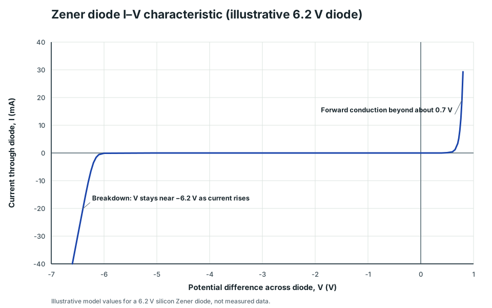
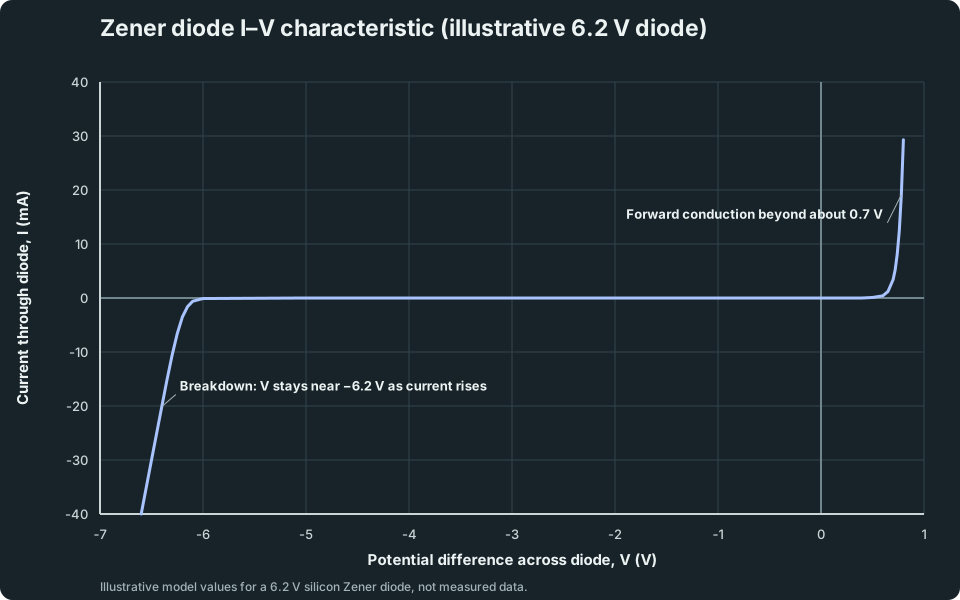
In a p-n junction diode, the reverse bias can be increased until the depletion layer breaks down and the diode suffers permanent damage. In a Zener diode, this does not happen because of a highly doped p-n junction. In a highly doped junction, the conduction and valence bands on opposite sides of the junction are sufficiently close during reverse bias such that electrons may tunnel directly from the valence band on the p-side into the conduction band on the n-side. When the reverse bias voltage passes beyond a critical magnitude known as the breakdown or Zener voltage, the entire depletion area is filled by the electrons migrating from the p to n-part of the barrier and any attempt to increase the voltage drop across the barrier is virtually unsuccessful.
Zener diode I–V characteristic (illustrative 6.2 V diode)
An I–V graph with forward bias positive. The forward current is negligible below about 0.6 V and rises steeply to about 30 mA by 0.8 V. In reverse bias the current is almost zero until about −6.1 V, then the curve drops almost vertically to −40 mA at −6.6 V.
Scroll across the graph to read all labels.
View figure data
| Potential difference across diode, V (V) | Current through diode, I (mA) |
|---|---|
| -6.6 | -40 |
| -6.5 | -30 |
| -6.4 | -20.1 |
| -6.35 | -15.2 |
| -6.3 | -10.6 |
| -6.25 | -6.6 |
| -6.2 | -3.5 |
| -6.15 | -1.6 |
| -6.1 | -0.6 |
| -6 | -0.1 |
| -5 | 0 |
| -3 | 0 |
| -1 | 0 |
| 0 | 0 |
| 0.4 | 0 |
| 0.5 | 0.1 |
| 0.6 | 0.4 |
| 0.65 | 1.2 |
| 0.7 | 3.4 |
| 0.72 | 5.2 |
| 0.74 | 8.1 |
| 0.76 | 12.4 |
| 0.78 | 19.1 |
| 0.8 | 29.3 |
The useful function is that the potential difference across the diode remains constant at VZ, over a wide range of reverse currents (i.e. the breakdown branch of the I–V characteristic is nearly vertical). It is this property of a Zener diode that makes it useful in stabilising power supplies, keeping the voltage output steady. Back To Solid State Physics
Treat V_Z as approximately constant only inside the stated operating current range. Outside that range, real-device non-ideal behaviour matters.
Next steps
Continue with the next resource in this course.
Course and syllabus information
- Course
- Advanced Physics
- Edition
- Advanced Physics