Semiconductors and NTC Thermistors
Key idea: Explain why semiconductor resistivity decreases with temperature and interpret the I–V characteristics of an NTC thermistor and semiconductor diode.
Continue where you stopped
The core idea
On this page
Learning objectives
- Apply resistance and resistivity, interpret I–V characteristics and explain temperature effects.
1. Semiconductor temperature dependence
A semiconductor has a number density of mobile charge carriers that increases strongly with temperature. Heating also increases lattice vibration and collisions, but the rise in carrier number density is the dominant effect for a typical semiconductor:
T↑ ⇒ n↑ ⇒ ρ↓.
This contrasts with a typical metal, where carrier number density is approximately constant and increased collision frequency makes resistivity rise with temperature.
For a metal, explain the trend using reduced drift velocity from more frequent collisions. For a semiconductor, explain it using the increased number density of charge carriers.
2. NTC thermistor
An NTC thermistor is a semiconductor component with a negative temperature coefficient: its resistance decreases as its temperature increases.
If self-heating is negligible and temperature is held constant, a thermistor can have an approximately linear I–V characteristic over a small range. In a typical measurement over a wider range, current heats the thermistor, lowering its resistance and making the curve become steeper.
3. Semiconductor diode
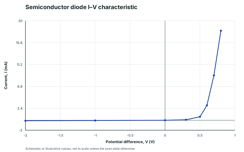
A diode conducts readily in its forward direction after the applied p.d. becomes sufficiently positive, but carries negligible reverse current in the idealised syllabus model.
Semiconductor diode I–V characteristic
An illustrative diode characteristic with negligible reverse current and a rapidly increasing forward current after the knee region.
Scroll across the graph to read all labels.
View figure data
| Potential difference, V (V) | Diode |
|---|---|
| -2 | -0.1 |
| -1 | -0.05 |
| 0 | 0 |
| 0.3 | 0.1 |
| 0.5 | 0.7 |
| 0.6 | 3 |
| 0.7 | 9 |
| 0.8 | 18 |
The precise curve depends on the diode material and temperature. Avoid claiming that every diode switches suddenly at exactly 0.7 V.
4. Comparing required I–V characteristics
| Component | Shape and symmetry | Physical reason |
|---|---|---|
| Ohmic resistor at constant temperature | straight line through origin; symmetric | constant resistance |
| Filament lamp | curve becomes less steep at large $ | V |
| NTC thermistor with self-heating | curve becomes steeper at large $ | V |
| Semiconductor diode | strongly asymmetric | conducts mainly in one direction |
5. Common Mistakes
- Explaining the semiconductor trend only as “electrons move faster”. The required cause is increased carrier number density.
- Reversing the temperature trends for a metal and an NTC thermistor.
- Treating an NTC thermistor as an ohmic resistor while its temperature is changing.
- Drawing a diode curve symmetric about the origin.
- Reading resistance directly as the gradient of an I–V graph; at a point, R = V/I.
6. Worked Examples
Modelled example 1
Compare a filament lamp and NTC thermistor
Problem
Study the worked solution
Explain the metal filament
Method
Link heating to greater resistance.Reason
Increased lattice vibration causes more frequent collisions and reduces drift velocity for a given field; carrier number density is approximately constant.Working
Metal: T↑ ⇒ collisions ↑ ⇒ ρ↑.Explain the NTC semiconductor
Method
Link heating to lower resistance.Reason
The large increase in mobile-carrier number density dominates the additional collisions.Working
NTC: T↑ ⇒ n↑ ⇒ ρ↓.Make the contrast explicit
Method
State that the dominant microscopic change differs.Reason
The two trends cannot be explained by temperature alone.Working
Metal: collision effect dominates; NTC: carrier-density effect dominates.
Guided practice 2
Identify a diode characteristic
Problem
Try this before viewing the solution
Hints
Hint 1: inspect symmetry
Hint 2: name the bias states
View solution step by step
Use the reverse region
Method
Identify blocking under reverse bias.Reason
The current is negligible for negative p.d.Working
Reverse bias: I ≈ 0.Use the forward region
Method
Identify ready conduction under forward bias.Reason
Current rises rapidly for positive p.d.Working
Forward bias: rapid increase in I.Name the component
Method
Conclude semiconductor diode.Reason
A diode’s I–V characteristic is strongly asymmetric.Working
Component: diode.
Common misconception 3
Why an NTC curve becomes steeper
Learner claim
Try this before viewing the solution
View solution step by step
Read the axes
Method
Use R = V/I at the operating point.Reason
On an I-against-V graph, I/V is conductance, not resistance.Working
R = V/I = 1/(I/V)Explain self-heating
Method
Link larger current to a hotter thermistor.Reason
Electrical power raises temperature during the measurement.Working
I↑ ⇒ heating ↑ ⇒ T↑.Apply the NTC mechanism
Method
Conclude that resistance falls.Reason
Heating greatly increases mobile-carrier number density.Working
T↑ ⇒ n↑ ⇒ ρ↓.
Examiner practice 4
Compare three non-ohmic characteristics
Examination question
Try this before viewing the solution
View solution step by step
Describe the lamp
1 markMethod
State symmetric and less steep at large |V|.Reason
Heating increases metal resistivity.Working
Lamp: symmetric; I grows less than proportionally with V.Describe the NTC thermistor
1 markMethod
State symmetric and steeper at large |V|.Reason
Heating increases carrier number density and lowers resistance.Working
NTC: symmetric; I grows more than proportionally with V.Describe the diode
1 markMethod
State strongly asymmetric.Reason
It blocks in reverse bias and conducts readily in forward bias.Working
Diode: negligible reverse current; rapid forward rise.State the comparison boundary
1 markMethod
Avoid assigning one universal turn-on voltage.Reason
The precise diode curve depends on material and temperature.Working
Use the curve shown or the stated diode model.
Self-mark with the mark scheme
Compare your response with each mark point. Select a point only when your response contains that evidence.
Self-mark the three curve descriptions and the diode-model qualification.
Challenge 5
Point resistance from a diode graph
Independent transfer
Try this before viewing the solution
Hints
Hint 1: convert the current
View solution step by step
Calculate the point ratio
Method
Divide voltage by current in amperes.Reason
R = V/I defines the ratio at the selected operating point.Working
V/I = 0.70/(9.0 × 10⁻³) = 78 ΩInterpret the curve
Method
Reject constant resistance.Reason
The diode curve is not a straight line through the origin, so V/I changes with operating point.Working
Different graph points give different V/I ratios.
7. Mind Stretchers
Mind stretcher 1: Temperature mechanisms without the comparison tableExtension
Explain, without referring back to the table, why heating makes a metal’s resistivity rise but a typical NTC semiconductor’s resistivity fall. State the microscopic quantity that dominates in each material.
Show Answer
In the metal, greater lattice vibration increases collision frequency and reduces drift velocity for a given field; carrier number density remains approximately constant, so resistivity rises. In the NTC semiconductor, the large increase in mobile-carrier number density dominates the additional collisions, so resistivity falls.
Next: Internal Resistance
Continue with the next resource in this course.
Course and syllabus information
- Course
- GCE A-Level H2 Physics
- Edition
- GCE A-Level H2 Physics 2027